


前提・実現したいこと
XilinxのVivadoと、DigilentのBASYS3を用いて、Microchip社のDAC,MCP4911を駆動するためのコードを書いています。
実現したい出力は、データシートの25ページ目、Figure 5-2の波形の、¬CS、SCK、SDIです。
Simulation上では想定通りの動作を確認しましたが、Generate Bitstreamの段階でCombination Loop Alertによりエラーが出てしまいます。
発生している問題・エラーメッセージ
[DRC LUTLP-1] Combinatorial Loop Alert: 1 LUT cells form a combinatorial loop. This can create a race condition. Timing analysis may not be accurate. The preferred resolution is to modify the design to remove combinatorial logic loops. If the loop is known and understood, this DRC can be bypassed by acknowledging the condition and setting the following XDC constraint on any one of the nets in the loop: 'set_property ALLOW_COMBINATORIAL_LOOPS TRUE [get_nets <myHier/myNet>]'. One net in the loop is c_SCK[0]. Please evaluate your design. The cells in the loop are: SCK_reg_i_5.
[DRC LUTLP-1] Combinatorial Loop Alert: 1 LUT cells form a combinatorial loop. This can create a race condition. Timing analysis may not be accurate. The preferred resolution is to modify the design to remove combinatorial logic loops. If the loop is known and understood, this DRC can be bypassed by acknowledging the condition and setting the following XDC constraint on any one of the nets in the loop: 'set_property ALLOW_COMBINATORIAL_LOOPS TRUE [get_nets <myHier/myNet>]'. One net in the loop is c_SCK[1]. Please evaluate your design. The cells in the loop are: SCK_reg_i_4.
[DRC LUTLP-1] Combinatorial Loop Alert: 1 LUT cells form a combinatorial loop. This can create a race condition. Timing analysis may not be accurate. The preferred resolution is to modify the design to remove combinatorial logic loops. If the loop is known and understood, this DRC can be bypassed by acknowledging the condition and setting the following XDC constraint on any one of the nets in the loop: 'set_property ALLOW_COMBINATORIAL_LOOPS TRUE [get_nets <myHier/myNet>]'. One net in the loop is c_SCK[2]. Please evaluate your design. The cells in the loop are: SCK_reg_i_3.
該当のソースコード
Verilog
1`timescale 1ns / 1ps 2 3module MCP4911_01a_main(clk,CSb,SCK,SDI); 4 input clk; 5 output reg CSb = 1; 6 output reg SCK = 0; 7 output reg SDI = 0; 8 9 reg bit15 = 0; 10 //0:Write to DAC register 11 //1:Ignore 12 13 reg BUF = 0; 14 //0:Unbuffered 15 //1:Buffered 16 17 reg GAb = 1; 18 //0:2x Vout 19 //1:1x Vout 20 21 reg SHDNb = 1; 22 //0:Shutdown the device 23 //1:Active 24 25 reg [9:0] D = 257; //data 26 27 reg [1:0] state = 0; 28 29 reg [7:0] count = 0; 30 31 reg [2:0] c_SCK = 0; //count to generate SCK/~SCK 32 reg [3:0] dig = 15; //16 digits 33 reg [7:0] dig_total = 47; //16 digits times 3 state equals 48 bits 34 wire [15:0] buff_SDI = {bit15,BUF,GAb,SHDNb,D,2'b00}; 35 wire [15:0] buff_SDI_start = 0; 36 wire [15:0] buff_SDI_end = 0; 37 reg f_gen_SCK = 0; //flag to generate SCK and ~SCK 38 39 always @(clk) begin 40 41 c_SCK <= c_SCK + 1; 42 43 if (c_SCK == 1) begin 44 case(state) 45 0: 46 SDI <= buff_SDI_start[dig]; 47 1: 48 SDI <= buff_SDI[dig]; 49 2: 50 SDI <= buff_SDI_end[dig]; 51 endcase 52 end else if (c_SCK == 7) begin 53 dig <= dig - 1; 54 dig_total <= dig_total - 1; 55 if (dig_total == 0) begin 56 dig_total <= 47; 57 end 58 if (dig == 0) begin 59 state <= state + 1; 60 if (state == 2) begin 61 state <= 0; 62 end 63 end 64 end 65 66 if (f_gen_SCK) begin 67 case (c_SCK) 68 7: SCK <= 0; 69 3: SCK <= 1; 70 endcase 71 end 72 73 case(dig_total) 74 32: CSb <= 0; 75 31: f_gen_SCK <= 1; 76 15: begin 77 f_gen_SCK <= 0; 78 CSb <= 1; 79 end 80 endcase 81 end 82 83endmodule
試したこと
代入の回数を減らすなどして、配線の干渉が起きにくくなるように工夫したが、エラーメッセージは変化しなかった
補足情報(FW/ツールのバージョンなど)
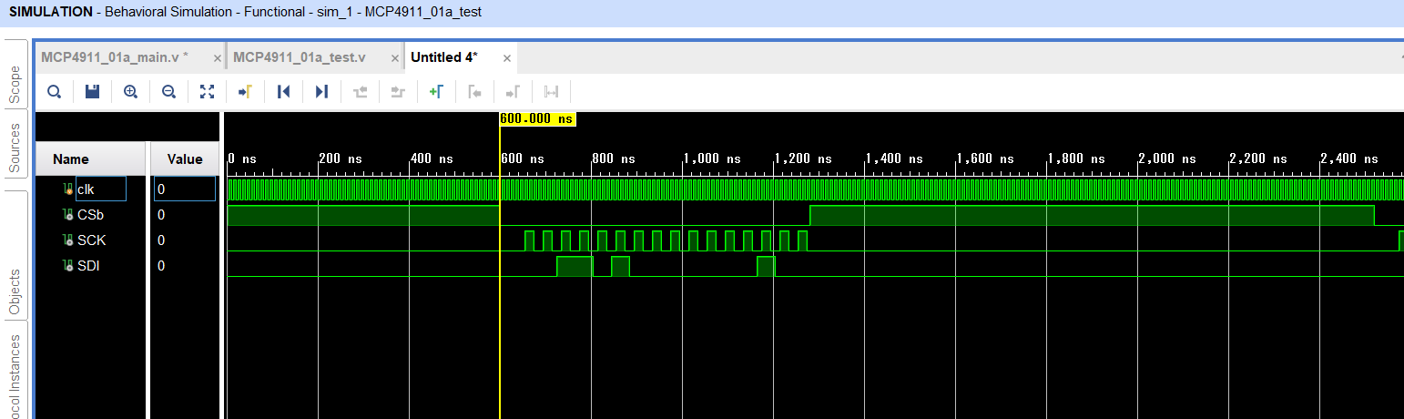
Simuration結果
FPGA: xc7a35tcpg236-1
ボード: BASYS 3
使用したいDAC: MCP4911
Vivado: v2019.1 (64-bit)
回答1件
あなたの回答
tips
プレビュー


バッドをするには、ログインかつ
こちらの条件を満たす必要があります。
2020/10/27 05:27 編集
2020/10/27 11:23